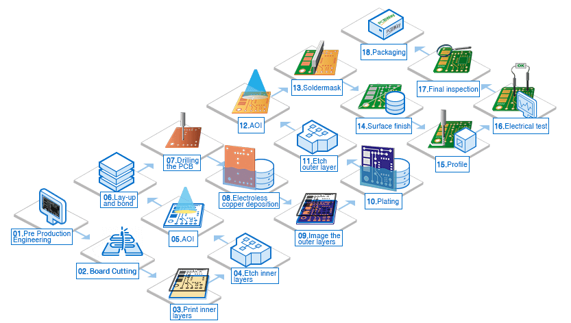
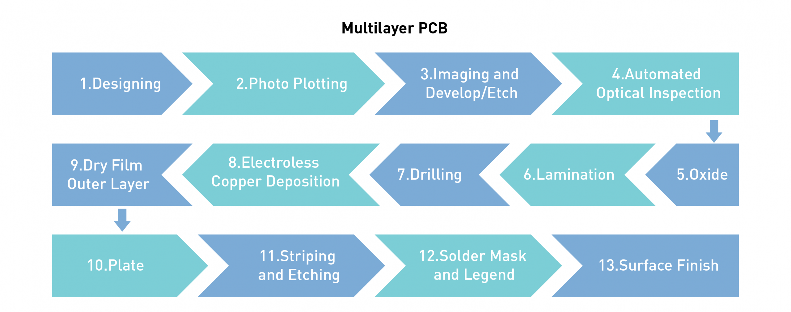
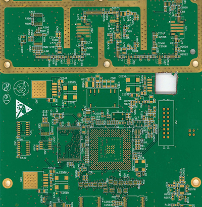
Multilayer Pcb Manufacturing Process Steps
Pcb Manufacturing Process Equipment Pcbway
Pcb Manufacturing Process News Season Multilayer Circuit Shenzhen Co Ltd

Multilayer Pcb Manufacturing Process Aipcba

Multilayer Pcb Manufacturing Process Steps Archives Electronics Tutorial The Best Electronics Tutorial Website
Multilayer Pcb Manufacturing Process A Tech Circuits

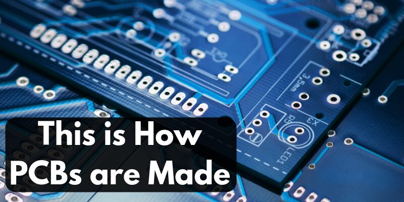
How Its Made Pcb Pcb Manufacturing Process Explained Youtube

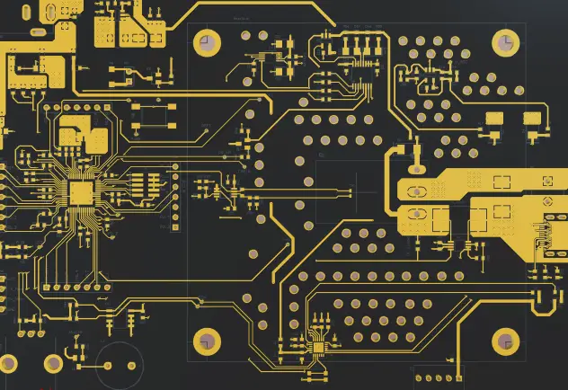
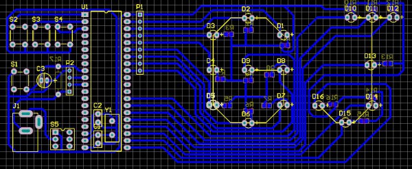
Designing the pcb step 2.
Multilayer pcb manufacturing process steps.

A Guide To The Pcb Manufacturing Process Mcl
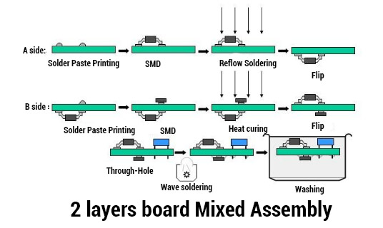
Printed Circuit Board Pcb Assembly Services Process Pcbway

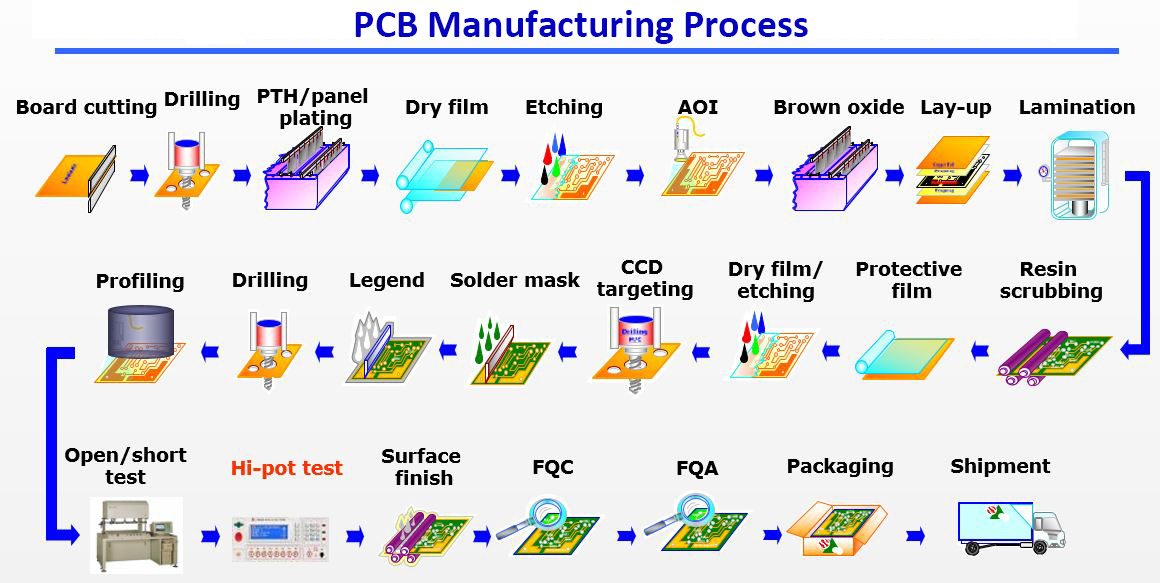
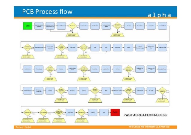
Pcb Manufacturing Process How Are Pcb Made Process Flowchart
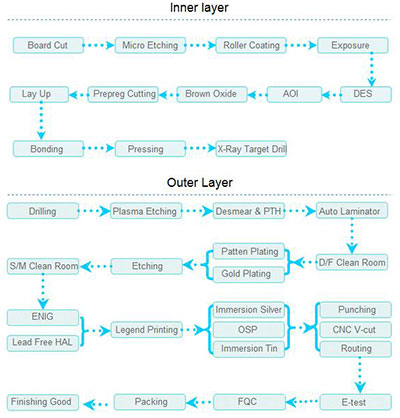
How To Manufacture Multilayer Pcb Moko Technology

Introduction To Multilayer Pcb Board Projectiot123 Technology Information Website Worldwide
Pcb Manufacturer Standard Pcb

The Manufacturing Steps Of Flex Circuit Boards Moko Technology

Rigid Pcb Design Manufacturing Benefits Types Of Pcb
Pcb Manufacturing How To Make A Pcb By Best Technology In China
Steps In Pcb Design And Manufacturing Tronicszone

Pcb Manufacturing Processes Viafine Pcb Limited
7 Problems In The Multilayer Pcb Fabrication Process
Pcb Manufacturing

Pcb Manufacture Process Synergy Electronics
Multilayer Pcb Manufacturing Process
Blog
Pcb Fabrication Process 20 Steps Ultimate Guide On Pcb Manufacturing

Pcb Fabrication Process What Are The Pcb Manufacturing Process Steps
Https Encrypted Tbn0 Gstatic Com Images Q Tbn And9gctnicpetgykewf54euuo9qn74idlvv5msu78krdh Xodopb2yg6 Usqp Cau
Wy2xnbhheb6xxm
Https Www Ncabgroup Com Wp Content Uploads 2016 12 Ncab Production Process How To Make A Pcb Pdf
Multilayer Pcb Ultimate Guide On Design And Manufacturing Process
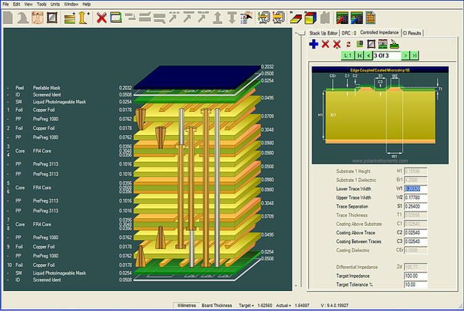
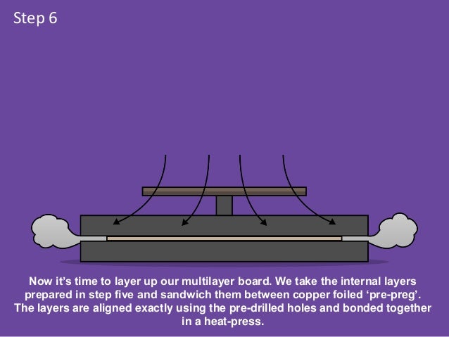
Sequential Lamination The Backbone Of Pcb Fabrication
Multilayer Printed Circuit Board Manufacturing Mrocess And Main Uses
Source : pinterest.com
